- 您现在的位置:买卖IC网 > Sheet目录3881 > PIC18F4539T-E/ML (Microchip Technology)IC PIC MCU FLASH 12KX16 44QFN
PIC18FXX39
DS30485A-page 130
Preliminary
2002 Microchip Technology Inc.
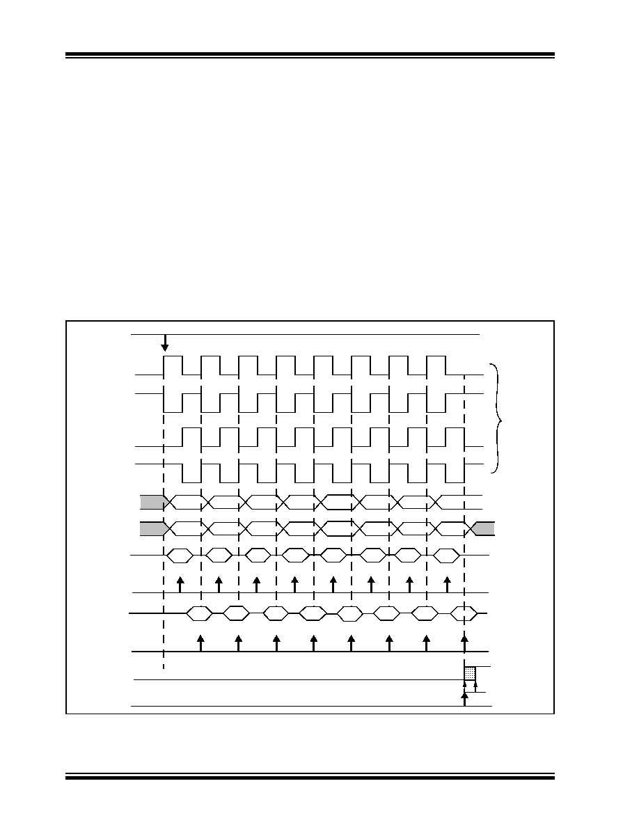
16.3.5
MASTER MODE
The master can initiate the data transfer at any time
because it controls the SCK. The master determines
when the slave (Processor 2, Figure 16-2) is to
broadcast data by the software protocol.
In Master mode, the data is transmitted/received as
soon as the SSPBUF register is written to. If the SPI is
only going to receive, the SDO output could be dis-
abled (programmed as an input). The SSPSR register
will continue to shift in the signal present on the SDI pin
at the programmed clock rate. As each byte is
received, it will be loaded into the SSPBUF register as
if a normal received byte (interrupts and status bits
appropriately set). This could be useful in receiver
applications as a “Line Activity Monitor” mode.
The clock polarity is selected by appropriately program-
ming the CKP bit (SSPCON1<4>). This then, would
give waveforms for SPI communication as shown in
MSB is transmitted first. In Master mode, the SPI clock
rate (bit rate) is user-programmable to be one of the
following:
FOSC/4 (or TCY)
FOSC/16 (or 4 TCY)
FOSC/64 (or 16 TCY)
This allows a maximum data rate (at 40 MHz) of
10.00 Mbps.
Figure 16-3 shows the waveforms for Master mode.
When the CKE bit is set, the SDO data is valid before
there is a clock edge on SCK. The change of the input
sample is shown based on the state of the SMP bit. The
time when the SSPBUF is loaded with the received
data is shown.
FIGURE 16-3:
SPI MODE WAVEFORM (MASTER MODE)
SCK
(CKP = 0
SCK
(CKP = 1
SCK
(CKP = 0
SCK
(CKP = 1
4 Clock
Modes
Input
Sample
Input
Sample
SDI
bit7
bit0
SDO
bit7
bit6
bit5
bit4
bit3
bit2
bit1
bit0
bit7
bit0
SDI
SSPIF
(SMP = 1)
(SMP = 0)
(SMP = 1)
CKE = 1)
CKE = 0)
CKE = 1)
CKE = 0)
(SMP = 0)
Write to
SSPBUF
SSPSR to
SSPBUF
SDO
bit7
bit6
bit5
bit4
bit3
bit2
bit1
bit0
(CKE = 0)
(CKE = 1)
Next Q4 cycle
after Q2
↓
发布紧急采购,3分钟左右您将得到回复。
相关PDF资料
PIC18LF8680T-I/PT
IC PIC MCU FLASH 32KX16 80TQFP
PIC16F1936-I/SO
IC PIC MCU FLASH 512KX14 28-SOIC
PIC18F24K20-I/SO
IC PIC MCU FLASH 8KX16 28SOIC
PIC18LF8585T-I/PT
IC PIC MCU FLASH 24KX16 80TQFP
XF2J-3024-11
CONN FPC 30POS 0.5MM SMT
PIC18LF6525T-I/PT
IC PIC MCU FLASH 24KX16 64TQFP
PIC18LF8621T-I/PT
IC PIC MCU FLASH 32KX16 80TQFP
PIC18F8620T-E/PT
IC PIC MCU FLASH 32KX16 80TQFP
相关代理商/技术参数
PIC18F4539T-E/PT
功能描述:8位微控制器 -MCU 24KB 1408 RAM 32 I/O RoHS:否 制造商:Silicon Labs 核心:8051 处理器系列:C8051F39x 数据总线宽度:8 bit 最大时钟频率:50 MHz 程序存储器大小:16 KB 数据 RAM 大小:1 KB 片上 ADC:Yes 工作电源电压:1.8 V to 3.6 V 工作温度范围:- 40 C to + 105 C 封装 / 箱体:QFN-20 安装风格:SMD/SMT
PIC18F4539T-I/ML
功能描述:8位微控制器 -MCU 24KB 1408 RAM 32 I/O RoHS:否 制造商:Silicon Labs 核心:8051 处理器系列:C8051F39x 数据总线宽度:8 bit 最大时钟频率:50 MHz 程序存储器大小:16 KB 数据 RAM 大小:1 KB 片上 ADC:Yes 工作电源电压:1.8 V to 3.6 V 工作温度范围:- 40 C to + 105 C 封装 / 箱体:QFN-20 安装风格:SMD/SMT
PIC18F4539T-I/PT
功能描述:8位微控制器 -MCU 24KB 1408 RAM 32 I/O RoHS:否 制造商:Silicon Labs 核心:8051 处理器系列:C8051F39x 数据总线宽度:8 bit 最大时钟频率:50 MHz 程序存储器大小:16 KB 数据 RAM 大小:1 KB 片上 ADC:Yes 工作电源电压:1.8 V to 3.6 V 工作温度范围:- 40 C to + 105 C 封装 / 箱体:QFN-20 安装风格:SMD/SMT
PIC18F4550EPT
制造商:Microchip Technology Inc 功能描述:
PIC18F4550-I/ML
功能描述:8位微控制器 -MCU 32kBF 2048RM FSUSB2 RoHS:否 制造商:Silicon Labs 核心:8051 处理器系列:C8051F39x 数据总线宽度:8 bit 最大时钟频率:50 MHz 程序存储器大小:16 KB 数据 RAM 大小:1 KB 片上 ADC:Yes 工作电源电压:1.8 V to 3.6 V 工作温度范围:- 40 C to + 105 C 封装 / 箱体:QFN-20 安装风格:SMD/SMT
PIC18F4550-I/P
功能描述:8位微控制器 -MCU 32kBF 2048RM FSUSB2 RoHS:否 制造商:Silicon Labs 核心:8051 处理器系列:C8051F39x 数据总线宽度:8 bit 最大时钟频率:50 MHz 程序存储器大小:16 KB 数据 RAM 大小:1 KB 片上 ADC:Yes 工作电源电压:1.8 V to 3.6 V 工作温度范围:- 40 C to + 105 C 封装 / 箱体:QFN-20 安装风格:SMD/SMT
PIC18F4550-I/PT
功能描述:8位微控制器 -MCU 32kBF 2048RM FSUSB2 RoHS:否 制造商:Silicon Labs 核心:8051 处理器系列:C8051F39x 数据总线宽度:8 bit 最大时钟频率:50 MHz 程序存储器大小:16 KB 数据 RAM 大小:1 KB 片上 ADC:Yes 工作电源电压:1.8 V to 3.6 V 工作温度范围:- 40 C to + 105 C 封装 / 箱体:QFN-20 安装风格:SMD/SMT
PIC18F4550T-I/ML
功能描述:8位微控制器 -MCU 32kBF 2048RM FSUSB2 RoHS:否 制造商:Silicon Labs 核心:8051 处理器系列:C8051F39x 数据总线宽度:8 bit 最大时钟频率:50 MHz 程序存储器大小:16 KB 数据 RAM 大小:1 KB 片上 ADC:Yes 工作电源电压:1.8 V to 3.6 V 工作温度范围:- 40 C to + 105 C 封装 / 箱体:QFN-20 安装风格:SMD/SMT